The Pulse
fJscaler Samples 100 GHz TIA for AI Datacenter Links
fJscaler says it is sampling a 100 GHz BiCMOS transimpedance amplifier to strategic customers for AI and cloud datacenter optical interconnects. The receiver targets 0.85 pJ/bit power efficiency, 18 pA/√Hz noise density and 200G-per-lane li
AI.info Team ·
fJscaler puts a 100 GHz receiver in customer sampling
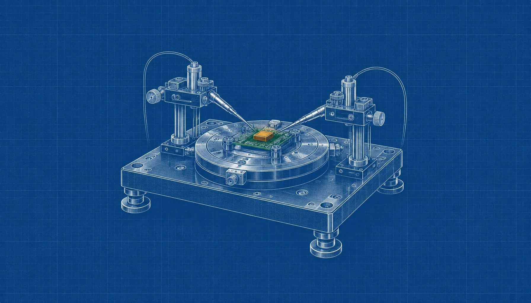
fJscaler is sampling a 100 GHz BiCMOS transimpedance amplifier to strategic customers, placing a high-speed receiver claim against a more immediate commercial test: whether module and system makers will adopt the device. The company announced the move on September 21, 2026, at ECOC 2026 in Málaga, Spain.
The component is designed for intensity-modulation direct-detection, or IM-DD, optical links used inside AI and cloud datacenters. fJscaler says the TIA reaches 0.85 picojoules per bit, an input-referred noise density of 18 pA/√Hz and 100 GHz of bandwidth.
Those figures, if reproduced in customer systems, would support 200G-per-lane and higher serial links while keeping receiver energy below one picojoule per bit. The company says the device is optimized for a back-illuminated indium phosphide photodiode, with a later version planned for silicon photonics receivers.
The bandwidth claim meets the power problem
Optical links are becoming a larger part of the power budget in very large AI clusters. Higher accelerator counts require more data to move between processors, memory and network equipment, but increasing link rates can raise the energy used by the optical electronics that send and receive those signals.
fJscaler’s approach targets the receiver front end rather than the entire optical system. A TIA converts the small electrical current from a photodiode into a usable voltage signal, making its noise, bandwidth and power consumption directly relevant to the quality and efficiency of the link.
“The economics of AI infrastructure are now written in picojoules per bit,” Jan Filip, fJscaler’s chief executive officer, said in the announcement. “Every fraction of a picojoule we remove from the optical link translates directly into more compute per watt and per dollar for our customers.”
From 100 GHz receivers to 1.6T optical systems
Filip said the TIA is intended to support the 1.6T and 3.2T generations of optical interconnects. The release connects the device to low-power, unretimed and linear-drive architectures, which reduce the amount of signal processing performed between the electrical and optical portions of a link.
The company’s 200G-per-lane target also reflects the direction of its earlier development work. In March 2025, fJscaler announced a 260 GBd BiCMOS linear-driver prototype for 1.6T coherent optics and 1.6T and 3.2T IM-DD applications. That earlier announcement described a 400G-per-lane path and said sampling to strategic partners would begin in the third quarter of 2025.
The new TIA addresses the receiving side of those systems. fJscaler says its BiCMOS design combines silicon-germanium speed with CMOS integration density, while placing the photodiode close to the receiver electronics reduces parasitic effects at the optical-electrical interface.
fJscaler adds photonic ICs for different reaches
Alongside the TIA, fJscaler announced a new family of photonic integrated circuits for 1.6T coherent-lite and IM-DD applications. The company positions coherent-lite for campus and inter-datacenter connections, where greater reach is needed, and IM-DD for shorter links inside datacenters.
“AI and cloud datacenters are driving an insatiable demand for bandwidth, and no single modulation approach covers every reach and cost point,” Samir Desai, a senior vice president at fJscaler, said in the release. He said the products are intended to give customers photonic ICs for both optical approaches alongside the company’s analog electronics.
Coherent-lite generally trades some of the reach and signal-processing capability of full coherent systems for lower power and cost. IM-DD remains attractive for shorter connections because its architecture is simpler, but it places greater pressure on the bandwidth and sensitivity of the transmitter and receiver components.
Sampling is the next test, not volume production
fJscaler says the 100 GHz BiCMOS TIA is sampling now to strategic customers. The announcement does not identify those customers, provide independent measurement data or set a date for general commercial availability.
That distinction matters for a component aimed at AI infrastructure. A laboratory bandwidth figure must translate into reliable operation with a photodiode, optical module, host system and link architecture before it becomes a product-level advantage. Customer sampling gives fJscaler a route to that validation, but the company’s announcement establishes availability for evaluation rather than broad deployment.
Marco Vitali, fJscaler’s chief technology officer, said the receiver was designed to preserve signal integrity at 200G per lane and above while supporting linear pluggable optics and co-packaged architectures. The next generation, he said, will extend the architecture to silicon photonics receivers.
The immediate product is therefore a receiver sample built around an InP photodiode. Its broader roadmap reaches toward silicon photonics, 1.6T coherent-lite and 3.2T optical systems, but those future applications are not the same as current production availability.