Future Horizons
Photonic and Neuromorphic Chips: The Post-Silicon Computing Race
Photonic and neuromorphic chips left the lab in 2026: Q.ANT signed IONOS as its first customer, Lightmatter joined NVIDIA's NVLink Fusion, Neurophos raised $110m. Silicon's answer, Maia 200, shipped in January.
Gabriele Masetti ·
The history of computing progress is, in large part, the history of making transistors smaller. Since Gordon Moore observed in 1965 that the number of transistors on a chip doubles roughly every two years, the semiconductor industry has sustained that trajectory through feats of engineering that border on the miraculous. Transistors today are measured in nanometres — a few dozen atoms wide. The factories that make them require the most precise manufacturing environments ever built by human beings.
But the laws of physics are not negotiable. Transistors are approaching the size of individual atoms, and quantum effects are beginning to undermine the reliable switching behaviour that computing depends on. Thermal dissipation is already a binding constraint: a modern GPU cluster running frontier AI workloads generates enough heat to require industrial cooling infrastructure. And energy consumption is becoming a geopolitical issue — the AI industry's electricity demands are measurable in the output of entire power plants.
Two radically different approaches to computing hardware are emerging in response to these limits: photonic computing, which uses light instead of electrical current to perform calculations, and neuromorphic computing, which uses chip architectures that mimic the structure and behaviour of biological neural networks. Neither is new as a concept — photonics research stretches back decades, and neuromorphic computing was named by Carver Mead at Caltech in 1990. What is new is that both are rapidly crossing the threshold from laboratory curiosity to commercial deployment, driven by the insatiable demand that AI has created for more efficient, more powerful computing substrates.
Why Silicon Is Running Out of Road
To appreciate why photonic and neuromorphic chips matter, it is worth being precise about what silicon-based computing is actually struggling with.
The fundamental bottleneck is not raw computational power. Modern GPUs can perform trillions of floating-point operations per second, and that number continues to grow. The bottleneck is the energy cost and physical heat generated by moving data. When a processor needs information from memory, it must move electrical signals through copper interconnects. That movement consumes energy and generates heat proportional to the volume of data moved and the distance it travels. As AI models grow larger — frontier systems are estimated to have well over a trillion parameters, and each generation grows further — the data movement problem becomes severe.
NVIDIA's H100 GPU, the workhorse of frontier AI training for years, has a thermal design power of 700 watts. A server rack of eight H100s consumes roughly the electricity of two average American households, continuously, at full load. A large training cluster of thousands of such GPUs consumes as much electricity as a small city.
The H100 is now two generations back, and the trend has gone the wrong way for anyone hoping the problem would solve itself. Blackwell Ultra parts shipped through 2025 at a substantially higher power envelope than Hopper, and NVIDIA launched the Vera Rubin platform at CES in January 2026, claiming eight times Blackwell's inference performance per watt. Performance per watt keeps improving; watts per GPU keep rising. None of that is sustainable at the scale the AI industry is targeting.
There is also a fundamental architectural mismatch between conventional computing hardware and neural networks. GPUs were designed for graphics rendering — a highly parallelisable workload that happens to suit neural network inference reasonably well. But the deep structure of neural networks, with their interconnected layers performing weighted summations and non-linear activations, is not ideally served by the von Neumann architecture that underlies all conventional chips. Every operation requires shuttling data between processing units and memory — a bottleneck so severe it has been given its own name: the memory wall.
Photonic Computing: Light-Speed Artificial Intelligence
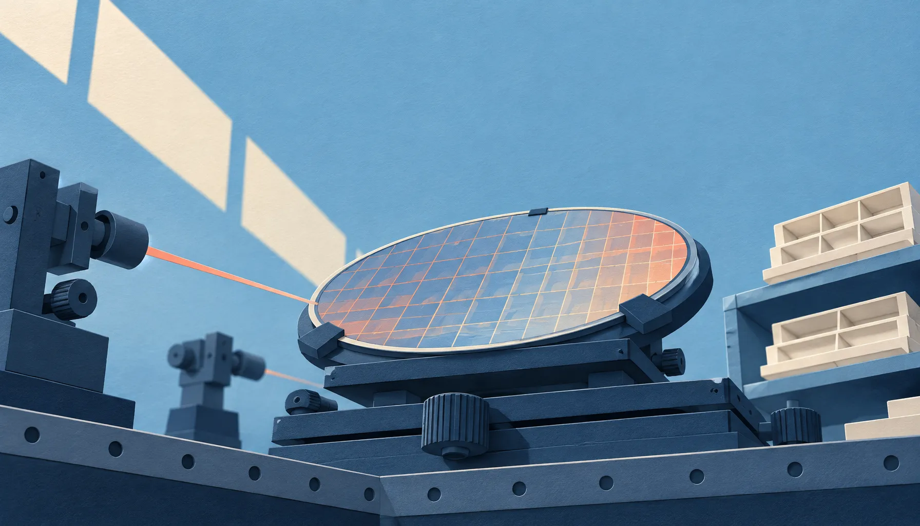
Photonic computing replaces electrical signals with photons — particles of light — to perform computation. That is not merely a metaphor for speed. The physics of photons give photonic computing a set of properties that are genuinely transformative for certain types of workloads.
Light travels through waveguides at, naturally, the speed of light. It generates essentially no heat as it propagates — photons do not interact with the crystal lattice of a material the way electrons do, so there is no resistive heating. Multiple beams of light can coexist in the same waveguide without interfering with each other if they are at different wavelengths, enabling a form of natural parallelism called wavelength-division multiplexing. And critically for AI: the mathematical operation at the heart of neural networks — the matrix multiplication — can be performed optically with extraordinary energy efficiency.
Matrix multiplication is the fundamental operation of neural network inference and training. Every layer of a neural network computes a weighted sum of its inputs, which is equivalent to multiplying a vector by a matrix. Photonic chips can perform this operation using the physical properties of light interference, in a single pass through an array of optical components, consuming a tiny fraction of the energy required by an equivalent electronic operation.
Q.ANT, a Stuttgart-based photonics company, claims 30 times lower energy consumption and 50 times higher throughput than conventional silicon for targeted AI workloads on its photonic processor. In May 2026 it named its first commercial customer: the German cloud provider IONOS, which took Q.ANT's Native Processing Server. A named paying customer is a different class of evidence from a benchmark claim, and it is the kind this field has been short of.
Lightmatter, a US photonics company, builds photonic interconnects aimed at the data-movement bottleneck in large GPU clusters, claiming 10 to 100 times better energy efficiency for inter-chip communication. On 2 June 2026 it joined NVIDIA's NVLink Fusion ecosystem, which is being extended to photonic interconnects, with mass production of its universal optical engine targeted for the first quarter of 2027. The incumbent is no longer ignoring the approach; it is absorbing it.
The rest of the field turns over quickly. Neurophos raised $110 million in January 2026 to build exaflop-scale photonic AI chips, while several earlier contenders have gone quiet — the ordinary attrition of a capital-intensive hardware category rather than a verdict on the physics.
| Chip | Type | Efficiency claim vs. conventional hardware |
|---|---|---|
| Intel Loihi 2 | Neuromorphic | 1,000-10,000x better energy efficiency (sparse, event-driven tasks) |
| IBM NorthPole | Neuromorphic | 22-25x better energy efficiency (image recognition benchmarks) |
| Q.ANT photonic processor | Neuromorphic-photonic hybrid | 30x lower energy, 50x higher throughput |
| Lightmatter | Photonic interconnect | 10-100x better efficiency (inter-chip communication) |
A team at the University of Florida demonstrated in 2025 that near-perfect accuracy in complex AI inference workloads could be achieved using an all-optical system — an important proof point that photonic approaches are not limited to simple or narrow tasks.
The key challenge for photonic computing remains the conversion overhead. The real world presents data as electrical signals. Converting those signals to optical form for computation, then converting back, consumes energy and introduces latency. For the photonic approach to win end-to-end, the gains in computation must outweigh the conversion costs. For large-scale matrix multiplications — exactly the operation that dominates AI workloads — the math increasingly favours the photonic approach.
Neuromorphic Computing: Chips That Think Like Brains
Neuromorphic computing takes a different approach to the silicon problem. Rather than replacing the physical medium of computation, it reimagines the architectural organisation of computing hardware to mirror the structure of biological neural networks.
The human brain performs cognitive tasks — pattern recognition, language understanding, sensory processing — with roughly 20 watts of power. The most energy-efficient large language model inference today requires several orders of magnitude more power per equivalent cognitive task. The brain achieves its efficiency through a combination of sparse activation (at any moment, most neurons are quiet), event-driven processing (neurons only fire when their input exceeds a threshold), and co-located memory and computation (synaptic weights are stored and applied locally, eliminating the memory wall).
Neuromorphic chips implement these principles in silicon. Instead of conventional transistors operating on floating-point numbers, they use spiking neural networks — artificial neurons that communicate through discrete pulses, or spikes, and only consume energy when they fire. Memory and processing are co-located at each artificial synapse, eliminating the energy cost of moving data between separate processing and memory units.
Intel's Loihi 2, released in 2021, remains the most widely studied neuromorphic processor, and Intel has not announced a public successor part. It contains 1 million artificial neurons and 120 million artificial synapses on a single chip, consumes under 1 watt for many tasks, and achieves 1,000 to 10,000 times better energy efficiency than conventional processors on the specific workloads it is designed for: sparse, event-driven pattern recognition tasks such as gesture detection, keyword spotting, and anomaly detection in sensor streams.
Intel's route has been to scale the same silicon rather than replace it. In April 2024 it assembled Loihi 2 chips into Hala Point, a research system with 1.15 billion artificial neurons — the largest neuromorphic computer built at the time, and a demonstration that the architecture survives being scaled up rather than only running well on a single die.
IBM's NorthPole chip, described in Science in 2023, takes a complementary approach: instead of spiking neurons, it uses a massively parallel array of small processing units each with local memory, eliminating off-chip memory access entirely for inference workloads. The results were striking — NorthPole achieved between 22 and 25 times better energy efficiency than comparable GPUs on standard image recognition benchmarks.
BrainChip's Akida processor is aimed at edge deployments — devices that need to perform AI inference locally, without cloud connectivity, on minimal power budgets. Akida is already deployed in automotive sensors, industrial monitoring equipment, and medical wearables. The company received the first commercial production batch of its AKD1500 processors in July 2026 and launched an AKD1500 PCIe evaluation card on 17 September 2026, which puts the chip into an ordinary desktop — a small step that matters for a category whose sharpest constraint is developer access. The market for edge AI inference, where energy budgets are measured in milliwatts rather than kilowatts, is where neuromorphic approaches have their clearest near-term competitive advantage.
The Convergence: Neuromorphic-Photonic Hybrids
The most ambitious approach at the frontier of hardware research combines both paradigms: photonic interconnects carry data between neuromorphic processing elements, creating chips that are simultaneously brain-inspired in their architecture and light-powered in their communication.
The Q.ANT NPU 2, mentioned above, is an early commercial example of this hybrid approach. Research groups at MIT, ETH Zurich, and several national laboratories are pursuing more radical versions: fully optical neuromorphic processors where both the storage of synaptic weights and the computation of neural activations are performed using light.
The theoretical performance ceiling for such systems is extraordinary. Optical matrix multiplications can in principle operate at terahertz clock rates — thousands of times faster than the gigahertz rates of conventional electronics. The energy consumption per operation would be a small fraction of the electronic equivalent. If the engineering challenges can be solved, a mature neuromorphic-photonic chip could offer the computational power of a current GPU cluster in a device the size of a postage stamp, running on a fraction of a watt.
The engineering challenges are significant. Fabricating reliable photonic components at nanometre scale is harder than fabricating electronic transistors. Optical components are sensitive to temperature variation in ways that electronic components are not. And the programming models for neuromorphic chips are fundamentally different from the standard deep learning frameworks — PyTorch and TensorFlow — that the AI industry has standardised on, creating a software ecosystem problem that must be solved alongside the hardware challenges.
The Geopolitical Dimension
The chip wars that have dominated AI geopolitics — the US export controls on advanced NVIDIA GPUs, the race to build domestic semiconductor capacity in Europe, Japan, and elsewhere — have been fought almost entirely on the terrain of conventional silicon.
Photonic and neuromorphic chips open a different competitive landscape. The manufacturing supply chains for photonic chips are less concentrated than those for advanced silicon — photonic waveguides can be fabricated using existing optical telecommunications infrastructure, which is distributed globally. That could reduce the strategic leverage Taiwan Semiconductor Manufacturing Company currently holds over the AI compute supply chain.
China, which has been largely cut off from advanced NVIDIA hardware by US export controls, has invested significantly in photonic and neuromorphic computing research as a potential bypass route. Several Chinese universities and state-backed companies are among the leaders in photonic AI accelerator research. If photonic approaches mature into viable alternatives to GPU-based computing, the chip war calculus changes substantially.
The European Union, which has struggled to establish a foothold in conventional semiconductor manufacturing, sees photonics as a strategic opportunity. The European Photonics Industry Consortium has identified AI photonics as a priority sector, and companies like Q.ANT, Multiverse Computing, and LightOn are building capabilities that could give Europe a competitive position in next-generation AI hardware.
What This Means for AI Capabilities
The practical question for the AI field is what photonic and neuromorphic chips unlock that silicon cannot.
In the near term — the next three to five years — the most significant impact is likely to be at the edge. Neuromorphic processors are already enabling AI applications that are impossible with conventional hardware on constrained power budgets: always-on keyword detection that runs for months on a coin cell battery, real-time anomaly detection in industrial sensors, medical monitoring devices that perform complex pattern recognition locally without transmitting sensitive data to the cloud. These are not headline-grabbing frontier AI capabilities, but they represent a significant expansion of where AI can operate.
In the medium term — five to ten years — photonic approaches could reduce the energy cost of large-scale AI inference by an order of magnitude or more. That would change the economics of AI deployment substantially: running a large language model could become cheap enough that every device and every application could afford continuous, personalised AI without the current reliance on expensive centralised cloud infrastructure.
In the longer term, if neuromorphic-photonic hybrid systems reach their theoretical potential, they could enable AI capabilities that are qualitatively different from today's — not merely faster versions of current systems, but systems with radically different memory structures, temporal processing characteristics, and energy envelopes. The brain's combination of energy efficiency, adaptability, and continuous learning from sparse data is not accidental; it reflects billions of years of optimisation under metabolic constraints. Computing systems that more closely mirror that architecture may unlock capabilities that the transformer architecture, optimised for silicon, cannot achieve.
The Timeline and the Risks
The cautious view, held by many mainstream hardware engineers, is that photonic and neuromorphic chips will remain niche solutions for specific workloads for the foreseeable future, while conventional silicon — supplemented by custom AI accelerators like Google's TPUs, Amazon's Trainium, and Microsoft's Maia — continues to dominate. The software ecosystem maturity, the manufacturing challenges, and the programming model differences all favour incumbents.
That case strengthened in 2026 rather than weakening. Microsoft launched Maia 200, a second-generation inference accelerator built on TSMC's 3-nanometre process with 216 gigabytes of HBM3e memory, on 26 January 2026, and Google and Amazon kept shipping their own parts on schedule. On delivered silicon, the cautious view is the one currently winning.
The more optimistic view, held by the companies and research groups actively building in this space, is that the energy and thermal constraints facing conventional AI hardware are severe enough to force a transition on a five-to-ten-year horizon. The economics are simple: as AI scales further, the energy costs of conventional hardware become unaffordable, and the first alternatives that offer comparable performance at a fraction of the power consumption will attract enormous investment and adoption.
Both views are defensible. What is clear is that the post-silicon computing race is no longer a distant academic prospect. Commercial products are shipping, venture capital is flowing, and governments are treating this as strategic infrastructure. The question is not whether the transition will happen, but how fast and who will lead it.
The Next Fifty Years of Computing
The transistor gave humanity five decades of exponential computing progress. The silicon-based era of AI is real and remarkable — but it is not the end of the story. It may not even be the middle.
Photonic chips offer the prospect of computing at the speed of light, with energy consumption a fraction of current silicon. Neuromorphic chips offer the prospect of computing that works the way biological intelligence works — sparse, event-driven, deeply efficient. Together, they point toward a future in which AI hardware is not measured by the number of GPU clusters it requires but by whether it can fit in a device you wear, deploy in a remote sensor, or run on the power budget of a small appliance.
The engineering challenges are real, and the timelines are uncertain. But the physics is sound, the investment is flowing, and the need is acute. The post-silicon computing race has begun in earnest, and its outcome will determine what kind of AI the second half of this century makes possible.