Technical Deep Dives
AI Hardware: GPUs, TPUs, and the Future of AI Compute
A guide to the silicon behind AI in 2026: NVIDIA's Rubin generation and its 288 GB of HBM4, Google's Ironwood TPU and the coming TPU 8 split, AWS Trainium3, and why bandwidth and interconnect, not FLOPS, set the pace.

Gabriele Masetti ·
Every leap in AI capability over the past decade has tracked a leap in compute hardware more closely than any leap in algorithms. Transformers existed as a paper in 2017; they became a product category only once GPUs and, later, custom accelerators made trillion-operation matrix multiplications routine at data-center scale. Understanding modern AI infrastructure means understanding a small number of chip families — NVIDIA's GPU line, Google's TPUs, and a growing set of inference-specialized accelerators — and the interconnect and numerical-precision tricks that let thousands of them work as one machine.
Why Matrix Multiplication Drives Chip Design
Neural network training and inference reduce, overwhelmingly, to matrix multiplications: the forward pass through a transformer layer is a sequence of matmuls between activations and weight matrices, and the backward pass computes gradients through more of the same operation. A general-purpose CPU executes this workload poorly because it is optimized for branching, low-latency scalar work, not for streaming millions of multiply-accumulate operations through wide, regular data paths.
GPUs happened to have already solved a similar problem for graphics rasterization, so NVIDIA's Volta architecture in 2017 introduced Tensor Cores — dedicated matrix-multiply units — as a bolt-on to the existing CUDA core array. Google took a more radical approach with the TPU, built from the outset around a systolic array, a grid of multiply-accumulate cells that pass partial sums directly to their neighbors without going back to memory between steps.
Both approaches converge on the same insight: the bottleneck for AI workloads is rarely raw arithmetic throughput, it is how fast operands can be fed to the arithmetic units, which is why memory bandwidth and interconnect speed dominate hardware roadmaps as much as FLOPS do.
NVIDIA's Data Center GPU Lineage
A100 (Ampere, 2020)
The A100, built on the Ampere architecture and unveiled in May 2020, was the accelerator that carried the first wave of large-scale transformer training. It shipped in 40 GB and 80 GB configurations using HBM2/HBM2e memory, with the 80 GB SKU reaching roughly 2 TB/s of memory bandwidth. Its third-generation NVLink provided up to 600 GB/s of GPU-to-GPU bandwidth, and its Tensor Cores delivered around 312 TFLOPS of dense FP16 throughput (624 TFLOPS with structured sparsity). It also introduced Multi-Instance GPU (MIG), partitioning one physical GPU into up to seven isolated instances — a feature that mattered as much for cloud economics as for raw performance.
H100 (Hopper, 2022)
NVIDIA announced the Hopper architecture and the H100 at GTC in March 2022, with volume shipments following in 2023. H100 moved to HBM3, delivering roughly 3.35 TB/s of memory bandwidth on the SXM module, and introduced fourth-generation NVLink at roughly 900 GB/s per GPU. The headline architectural addition was native FP8 support in the Tensor Cores, alongside a Transformer Engine that dynamically manages precision during training.
On a per-GPU basis, H100 reaches roughly 1,980 TFLOPS of dense FP8 (about 3,960 TFLOPS with sparsity) — double the throughput of the equivalent BF16 operation. Demand for H100 in 2023 was severe enough that it became the primary supply bottleneck for nearly every large training run announced that year.
H200 (Hopper refresh, 2024)
H200, which reached general availability in mid-2024, kept the Hopper compute architecture unchanged and instead re-based the GPU on 141 GB of HBM3e, lifting memory bandwidth to roughly 4.8 TB/s. That is a memory-only upgrade — the FP8 and FP16 Tensor Core throughput figures are essentially the same as H100's — but for inference bound on weight residency and KV-cache size, more memory and bandwidth translate directly into higher throughput without any compute increase.
Blackwell: B200 and GB200 (2024–2025)
NVIDIA revealed the Blackwell architecture at GTC in March 2024. The flagship B200 GPU module departs from the single-die designs of Ampere and Hopper: it fuses two reticle-limited dies into one package over a 10 TB/s die-to-die link, presenting to software as a single GPU. B200 carries 192 GB of HBM3e and roughly 8 TB/s of aggregate memory bandwidth — more than double H100's.
Fifth-generation NVLink raises per-GPU interconnect bandwidth to 1.8 TB/s (18 links running at 100 GB/s each, versus H100's 900 GB/s). Blackwell also introduces native FP4 and FP6 support with the per-block "micro-scaling" formats (MXFP4/MXFP6/MXFP8) described below.
B200's dense FP4 throughput reaches roughly 9 PFLOPS (18 PFLOPS with sparsity) — about double its own FP8 rate. The Grace Blackwell GB200 superchip pairs two B200 GPUs with a Grace CPU over a 900 GB/s NVLink-C2C chip-to-chip link, and the rack-scale GB200 NVL72 configuration links 72 Blackwell GPUs through NVLink Switch fabric for roughly 130 TB/s of all-to-all bandwidth in one liquid-cooled rack — effectively one very large accelerator, for training and above all for low-latency inference.
Blackwell Ultra: B300 (2025)
The Blackwell Ultra B300, NVIDIA's mid-cycle refresh, adds roughly 50% more memory over B200 — 288 GB of HBM3e — while pushing dense FP4 throughput to roughly 15 PFLOPS, at a higher 1,400 W TDP per GPU. GB300 NVL72 racks pair 72 B300 GPUs with 36 Grace CPUs, continuing the emphasis on inference-heavy deployments where memory capacity for KV-caches and mixture-of-experts weights, rather than raw FLOPS, is often the binding constraint.
Rubin (2026)
Rubin, announced at CES in January 2026, displaced Blackwell Ultra at the top of the line. NVIDIA put the platform into full production in June 2026, CoreWeave completed the first Vera Rubin NVL72 bring-up the same month, and the racks now run at Google Cloud, Microsoft Azure and Oracle Cloud Infrastructure.
A Rubin GPU carries up to 288 GB of HBM4 at roughly 22 TB/s — about 2.8 times Blackwell's memory bandwidth — and NVIDIA rates it at 50 PFLOPS of NVFP4 compute for inference. Sixth-generation NVLink doubles per-GPU interconnect bandwidth again to 3.6 TB/s, and the Vera Rubin NVL72 rack, 72 Rubin GPUs with 36 Vera CPUs, reaches 260 TB/s of aggregate scale-up bandwidth. NVIDIA's headline comparisons are economic: a tenfold cut in the cost of generating an inference token against Blackwell, and four times fewer GPUs to train a mixture-of-experts model.
Google's TPU Lineage: Systolic Arrays at Scale
Google's Tensor Processing Units have followed a parallel but architecturally distinct path, alternating between "performance" chips optimized for large training runs and "efficiency" chips optimized for cost-per-token at inference and mid-scale training.
TPU v4, deployed from 2021, arranged chips in a 3D torus topology and scaled pods to several thousand chips, giving Google enough aggregate throughput to train its largest models of that era without relying on merchant GPU supply. TPU v5e, announced in 2023, is explicitly the cost-efficient member of the fifth generation: each chip delivers around 393 trillion INT8 operations per second, uses a simpler 2D torus topology, and is designed to scale to pods of 256 chips rather than the largest possible cluster.
TPU v5p, announced in December 2023 as the performance-oriented fifth-generation chip, roughly doubles the per-chip compute of v5e, carries 95 GB of HBM per chip at 2,765 GB/s of bandwidth, and was benchmarked by Google at 2.8x faster large-model training than TPU v4.
Trillium, the sixth-generation TPU (v6e), was announced at Google I/O in May 2024 and reached general availability later that year. Trillium expands the matrix-multiply unit to a 256x256 array, larger than prior generations, and Google reports over 4x the training performance and up to 3x the inference throughput of v5e, a 67% improvement in energy efficiency, and double the HBM and inter-chip interconnect (ICI) bandwidth.
Ironwood, the seventh-generation TPU, was previewed at Google Cloud Next in April 2025 but became generally available only a year later, on 22 April 2026, at Cloud Next 2026. It is Google's first TPU explicitly positioned around inference at scale rather than training, with per-chip specifications of roughly 4,614 FP8 TFLOPS, 192 GB of HBM3e, 7.37 TB/s of memory bandwidth, and 9.6 Tb/s of inter-chip interconnect. A single superpod links 9,216 chips for 42.5 EFLOPS. Those per-chip numbers sit in the same class as NVIDIA's Blackwell generation, reached from an entirely different architecture.
At the same event Google previewed an eighth generation and, for the first time, split it in two: TPU 8t, codenamed Sunfish, a training chip co-designed with Broadcom, and TPU 8i, codenamed Zebrafish, a single-die inference chip co-designed with MediaTek at a lower unit cost. Both use TSMC's 2 nm process and are targeted at late 2027, and a Sunfish superpod is specified at 9,600 chips, 2 PB of HBM and 121 EFLOPS of FP4 compute.
| Chip | Maker | Dense throughput | Memory | Bandwidth |
|---|---|---|---|---|
| Ironwood (TPU v7) | ~4,614 FP8 TFLOPS | 192 GB HBM3e | 7.37 TB/s | |
| B200 (Blackwell) | NVIDIA | ~9 PFLOPS dense FP4 | 192 GB HBM3e | ~8 TB/s |
| Rubin | NVIDIA | ~50 PFLOPS NVFP4 (inference) | 288 GB HBM4 | ~22 TB/s |
The HBM Bandwidth Race
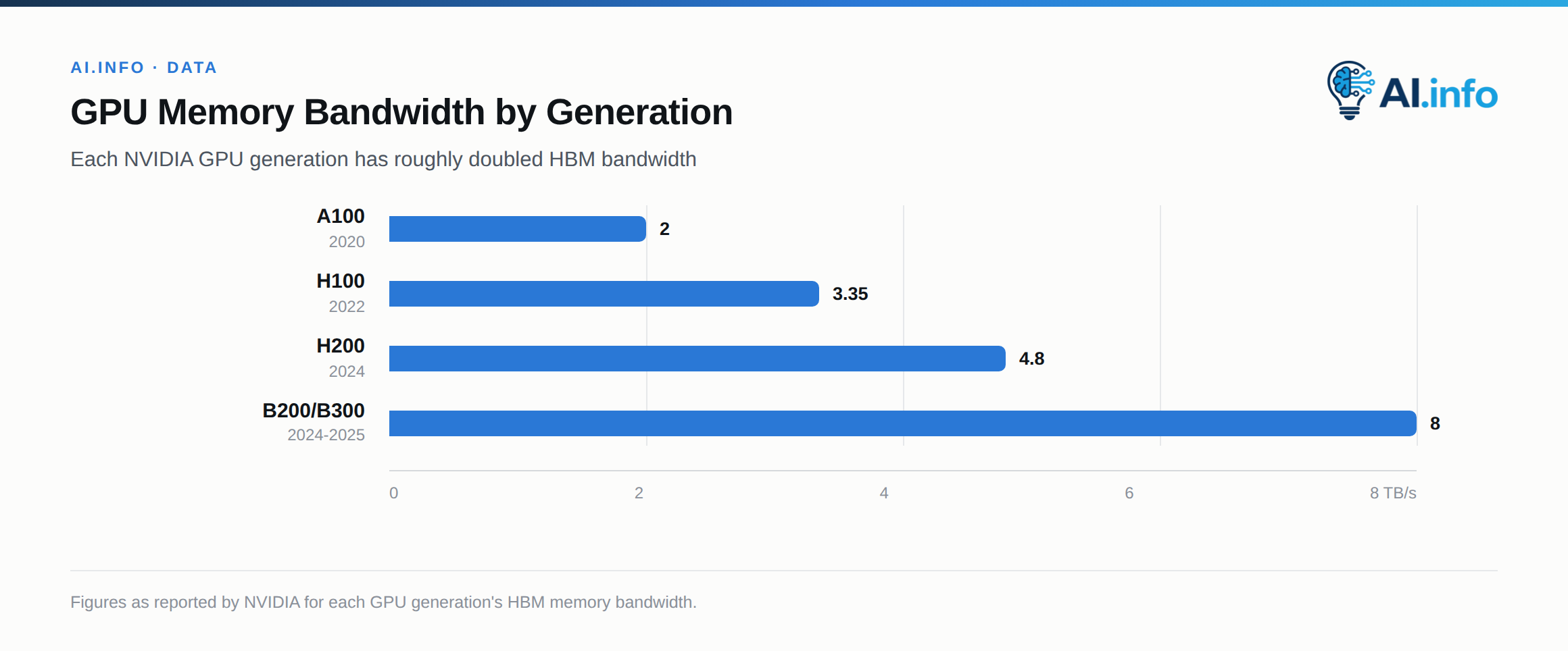
Across every one of these lineages, memory bandwidth has scaled faster than compute, because attention mechanisms and large parameter counts are frequently memory-bound rather than compute-bound at inference time. The progression is stark: A100's roughly 2 TB/s, H100's 3.35 TB/s, H200's 4.8 TB/s, B200/B300's roughly 8 TB/s and Rubin's roughly 22 TB/s all use successive generations of High Bandwidth Memory (HBM2e, HBM3, HBM3e, HBM4) stacked directly on the same package as the compute die via silicon interposers.
On the TPU side, Ironwood's 7.37 TB/s per chip and Trillium's doubled bandwidth over v5e show the same trend. HBM capacity is as contested a resource as the compute itself: supply constraints at SK Hynix, Samsung and Micron have at various points throttled how many accelerators NVIDIA and Google could ship, independent of fab capacity for the logic die.
Interconnect: Scaling Beyond One Chip
No single accelerator, however capable, trains a frontier model alone. NVLink is NVIDIA's proprietary chip-to-chip interconnect for scale-up communication within a node or rack: third-generation NVLink on A100 provided 600 GB/s, fourth-generation on H100 raised that to roughly 900 GB/s, fifth-generation on Blackwell doubled per-GPU bandwidth to 1.8 TB/s, and NVLink 6 on Rubin doubles it once more to 3.6 TB/s.
NVSwitch chips extend NVLink into an any-to-any fabric across many GPUs in a rack; in the GB200/GB300 NVL72 systems this fabric delivers roughly 130 TB/s of aggregate bandwidth across 72 GPUs, and 260 TB/s in Vera Rubin NVL72. Once a workload needs to span multiple racks or an entire data-center pod, NVIDIA hands off to InfiniBand (via its Quantum switch line) or Ethernet-based fabrics for scale-out networking, which trade some latency and bandwidth for the ability to connect tens of thousands of GPUs.
Google's TPU pods use their own inter-chip interconnect (ICI) for a similar scale-up role, with optical circuit switches used to reconfigure pod topology at multi-thousand-chip scale. Scale-up (inside a rack, NVLink/ICI) and scale-out (between racks, InfiniBand/Ethernet) are deliberately different technologies with different bandwidth-latency tradeoffs, and getting that hierarchy right matters more to real training throughput than the peak FLOPS of any single chip.
Precision: FP16 to FP8 to FP4
The numerical precision used for matrix multiplication has fallen with each hardware generation, driven by the observation that neural networks tolerate substantial quantization noise, especially at inference time. Ampere-generation Tensor Cores ran primarily FP16/BF16 and TF32; Hopper's H100 introduced native FP8 support in the Tensor Cores plus a Transformer Engine to manage mixed precision automatically, roughly doubling matmul throughput over BF16 at equivalent power.
Blackwell went a generation further, adding native FP6 and FP4 support with fine-grained micro-scaling formats (MXFP8, MXFP6, MXFP4) where a shared exponent scale applies to blocks of around 32 values rather than an entire tensor — a change that recovers much of the dynamic range lost when dropping to 4 bits per value. Those formats are now the unit everyone quotes: NVIDIA rates Rubin in NVFP4, and AWS built MXFP8 and MXFP4 into Trainium3.
The effect compounds: FP4 is roughly double FP8 on Blackwell, and FP8 was already double BF16 on Hopper, so a Blackwell GPU running FP4 inference offers on the order of 4x the raw throughput of an H100 running FP8 — for workloads that tolerate the loss, typically post-training-quantized inference rather than training, where higher precision is still used for numerical stability.
Inference-Specialized Silicon
Training-optimized GPUs and TPUs run inference too, but a distinct category of chips trades training flexibility for inference latency and cost. Groq's LPU (Language Processing Unit) used a deterministic, compiler-scheduled architecture built around enormous on-chip SRAM bandwidth rather than off-chip HBM, removing the memory-access unpredictability that causes latency jitter on GPUs, and ran Llama-class models at hundreds of tokens per second per user.
The argument was persuasive enough that NVIDIA bought it rather than beat it. On 24 December 2025 NVIDIA agreed to acquire Groq's assets and licence its LPU technology non-exclusively for about $20 billion, the largest deal on its record, hiring Groq's founder and part of the team. What emerged is an annexe to the GPU rather than a competitor. The NVIDIA Groq 3 LPX rack, in full production since August 2026, holds 256 LPU accelerators, each with 500 MB of on-chip SRAM at 150 TB/s, for 128 GB of SRAM and 40 PB/s per rack. It sits beside a Vera Rubin NVL72 and splits the work by phase — the GPUs compute the bandwidth-heavy context, the LPUs generate the tokens — for up to 35x more tokens per watt at extreme speeds than Blackwell NVL72 alone, by NVIDIA's figures.
| Chip | Vendor | Role | Key figure |
|---|---|---|---|
| Groq 3 LPU | NVIDIA (Groq IP) | Inference decode | 500 MB SRAM at 150 TB/s per chip |
| Trainium3 | AWS | Training | 2.52 PFLOPS FP8, 144 GB HBM3e, 4.9 TB/s |
| Inferentia2 | AWS | Inference | ~190 TFLOPS FP16, 32 GB HBM |
AWS has taken a different path with its own silicon. Trainium2 underpins Project Rainier: the New Carlisle site held roughly 500,000 chips when it came online in October 2025, and by April 2026 Anthropic said it was using more than one million Trainium2 chips to train and serve Claude, with nearly 1 GW of combined Trainium2 and Trainium3 capacity due online across AWS by the end of 2026.
Trainium3 arrived at re:Invent in December 2025, when AWS declared Trn3 UltraServers generally available. It is the company's first 3 nm AI chip, rated at 2.52 PFLOPS of FP8 per chip with 144 GB of HBM3e at 4.9 TB/s, and it ships MXFP8 and MXFP4 rather than promising them; an UltraServer scales to 144 chips for 362 FP8 PFLOPS, up to 4.4x the compute of Trainium2. Inferentia2, AWS's dedicated inference chip, offers around 190 TFLOPS of FP16 throughput with 32 GB of HBM per accelerator, at substantially lower cost per inference than the first-generation Inferentia it replaced.
Reading the Roadmap
The pattern across these product lines is consistent enough to be predictive: each generation adds a lower-precision numeric format, roughly doubles memory bandwidth via a newer HBM standard, and roughly doubles scale-up interconnect bandwidth, while die-level compute growth comes from packaging multiple dies together rather than single-die scaling, because reticle limits cap how large one lithography exposure can be.
The 2026 generation followed that script and added a move to it. Rubin, Trainium3 and Ironwood arrived within months of each other with micro-scaled formats, more HBM and faster fabric. What is new is specialization by phase: Google split its eighth-generation TPU into a training chip and an inference chip, NVIDIA bolted an SRAM-based decode accelerator onto its GPU racks, and Ironwood was built for serving from the start. Prefill and decode have different bottlenecks, and the industry has stopped asking one die to absorb both.
For anyone building or buying AI infrastructure, the operative question is rarely which chip has the highest advertised FLOPS — it is which combination of memory bandwidth, interconnect topology, and supported precision best matches a specific workload's actual bottleneck, since training a frontier model and serving low-latency inference for it stress almost entirely different parts of the same hardware stack.